80386 microprocessor pin diagram
Home » Background » 80386 microprocessor pin diagramYour 80386 microprocessor pin diagram images are available. 80386 microprocessor pin diagram are a topic that is being searched for and liked by netizens now. You can Get the 80386 microprocessor pin diagram files here. Get all free vectors.
If you’re looking for 80386 microprocessor pin diagram pictures information linked to the 80386 microprocessor pin diagram interest, you have pay a visit to the right blog. Our website always provides you with suggestions for seeing the maximum quality video and picture content, please kindly search and locate more informative video content and images that match your interests.
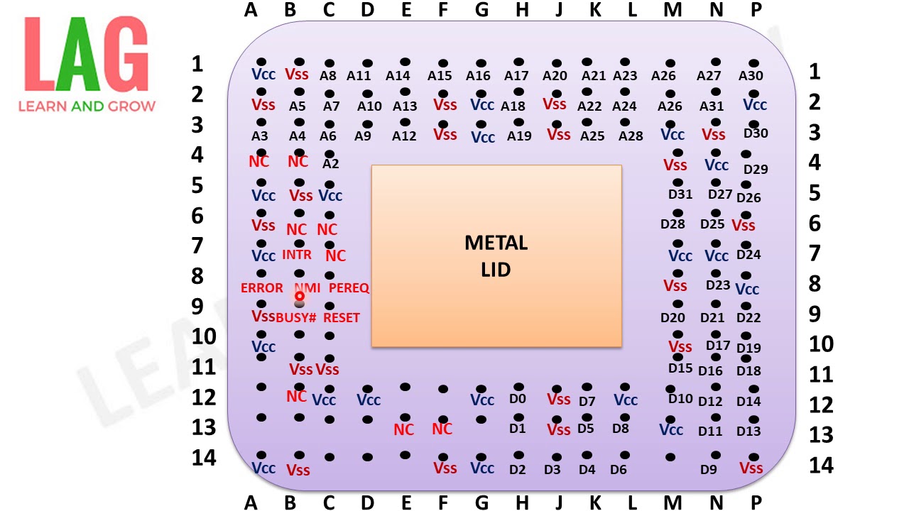
80386 Microprocessor Pin Diagram. INTRODUCTION TO THE 80386 MICROPROCESSOR. You can Google it and you will get hundreds of result you can select which you think is the most appropriate for you. Introduction to the 80386 Microprocessor the 80386DX is packaged in a 132-pin PGA. Figure 171 illustrates the pin-out of the 80386DX.
 Architecture Of 80386 Microprocessor Youtube From youtube.com
8086 is a 16-bit microprocessor and was created by Intel in 1978. Introduction to the 80386 Microprocessor the 80386DX is packaged in a 132-pin PGA. These lines constitute the time multiplexed memoryIO address during the first clock cycle T1 and data during T2 T3 and T4 clock cycles. We can see this under the heading The 8086 Microprocessor- Internal ArchitectureThe 80186 is 68 pins lead-less package so it has enough pins to send out both the minimum mode type signals RD and WR and the S0 S3 status signals which can be connected to external bus controller ICs for maximum mode systems. Introduction to 80386dx Architecture. Just like the 80386 the 32-bit address bus of the 80486 enabled up to 4 Gigabyte of memory to be directly addressed using a flat memory model with 32-bit linear addresses in protected mode.
However unlike the 8085 microprocessor an 8086 to have better performance operates in 2 modes that are.
Unlike in real mode the selector has nothing to. It is available in 40 pin DIP chip. Interfaces of the 80386DX Four interfaces MemoryIO interface Interrupt Interface DMA. Architecture of 80386 microprocessor. Module The Intel Microprocessors 80868088 Architecture consists of the following subtopics 80868088 CPU Architecture Programmers Model Functional Pin Diagram Memory Segmentation Banking in 8086 Demultiplexing of AddressData bus Study of. Brey Figure 133 The 8237A-5 programmable DMA controller.
 Source: pt.slideshare.net
Successive 16 bit bus cycles may be executed to read a 32 bit data from a peripheral. To make room for the additional signals the 80486 is packaged in a 168 pin pin grid array package instead of the 132 pin PGA used for the 80386. Pin Diagram and Description of 8086 Microprocessor. Diagram 1 mark and Explanation 3 marks A protected-mode segment register holds a 16-bit segment selector see the figure below. Signal Pin Numbering Lect 12-4.
 Source: slidetodoc.com
AD0 - AD15 IO. Internal Architecture of the 80486. The 20 lines of the address bus operate in multiplexed mode. Interfaces of the 80386DX Block Diagram of the 80386 Lect 12-5. 80386DX addresses 4G bytes of.
 Source: pdfprof.com
Just like the 80386 the 32-bit address bus of the 80486 enabled up to 4 Gigabyte of memory to be directly addressed using a flat memory model with 32-bit linear addresses in protected mode. Brey Figure 133 The 8237A-5 programmable DMA controller. A31 to A2 - Address bus connections address any of the 4G bytes memory locations in the 80386 memory system. Architecture of 80386 microprocessor. The Intel 386 originally released as 80386 and later renamed i386 is a 32-bit microprocessor introduced in 1985.
 Source: slideplayer.com
Just like the 80386 the 32-bit address bus of the 80486 enabled up to 4 Gigabyte of memory to be directly addressed using a flat memory model with 32-bit linear addresses in protected mode. INTRODUCTION TO THE 80386 MICROPROCESSOR. Architecture of 80386 microprocessor. Intel 8086 is a 16-bit HMOS microprocessor. BS16The bus size 16 input pin allows the interfacing of 16 bit devices with the 32 bit wide 80386 data bus.
 Source: researchgate.net
Architecture of 80386 microprocessor. Brey Figure 133 The 8237A-5 programmable DMA controller. AD0 - AD15 IO. Figure 171 illustrates the pin-out of the 80386DX. The Intel 386 originally released as 80386 and later renamed i386 is a 32-bit microprocessor introduced in 1985.
 Source: researchgate.net
Interfaces of the 80386DX Four interfaces MemoryIO interface Interrupt Interface DMA. Figure-1 depicts pin diagram of 8086 and 80286. As the original implementation of the 32-bit extension of the 80286 architecture the i386 instruction set programming model and binary encodings are. INTRODUCTION TO THE 80386 MICROPROCESSOR. Following are the features of 80386 microprocessor.
 Source: pt.slideshare.net
Krishna Kumar MAMM8LU18V12004 7 Signal Descriptions of 80386 cont CLK2 The input pin provides the basic system clock timing for the operation of 80386. It is available in 40 pin DIP chip. You can Google it and you will get hundreds of result you can select which you think is the most appropriate for you. This section of the chapter details the operation of each pin along with the external memory system and IO structures of the 80386. These are upper 30 bit of the 32- bit address bus.
 Source: in.pinterest.com
The 486 has a 32-bit data bus and a 32-bit address bus. 80486 is an 8Kbyte code and data cache. The bus hold input pin enables the other bus masters to gain control of the system bus if it is asserted. 386 DX Microprocessor Flexible 32-bit Microprocessor. BS16The bus size 16 input pin allows the interfacing of 16 bit devices with the 32 bit wide 80386 data bus.
Source:
Pin description of 80486. The 20 lines of the address bus operate in multiplexed mode. Internal Architecture of the 80486. Figure 171 illustrates the pin-out of the 80386DX. 8086 is a 16-bit microprocessor and was created by Intel in 1978.
 Source: youtube.com
BS16The bus size 16 input pin allows the interfacing of 16 bit devices with the 32 bit wide 80386 data bus. AD0 - AD15 IO. Function of each 80386dx group of pins. Q1v With the neat diagram describe the selector fields in 80386 microprocessor 4 Ans. Pin Diagram and Pin description of 8086.
 Source: slidetodoc.com
Diagram 1 mark and Explanation 3 marks A protected-mode segment register holds a 16-bit segment selector see the figure below. Pin Description of 80386dx. The CLKOUT pin drives other devices in a system and provides a timing source to additional microprocessors in the system. Courtesy of Intel Corporation. The 8086 uses 20-line address bus.
 Source: slideserve.com
Before the 80386 or any other microprocessor can be used in a system the function of each pin must be understood. 80486 is an 8Kbyte code and data cache. Signal Pin Numbering Lect 12-4. You can Google it and you will get hundreds of result you can select which you think is the most appropriate for you. AD0 - AD15 IO.
Source: youtube.com
Unlike in real mode the selector has nothing to. Introduction to the 80386 Microprocessor the 80386DX is packaged in a 132-pin PGA. To make room for the additional signals the 80486 is packaged in a 168 pin pin grid array package instead of the 132 pin PGA used for the 80386. The CLKOUT pin drives other devices in a system and provides a timing source to additional microprocessors in the system. Diagram 1 mark and Explanation 3 marks A protected-mode segment register holds a 16-bit segment selector see the figure below.
 Source: researchgate.net
The 16-low order address bus lines have been. Like the pin configuration of 8085 microprocessor the 8086 microprocessor also contains 40 pins dual in line. It is available in 40 pin DIP chip. Interfaces of the 80386DX Block Diagram of the 80386 Lect 12-5. Before the 80386 or any other microprocessor can be used in a system the function of each pin must be understood.
 Source: electronicsdesk.com
Internal Architecture of the 80486. Pin Diagram and Pin description of 8086. Times as fast as a 80386387 combination. Introduction to 80386dx Architecture. 80486 is an 8Kbyte code and data cache.
 Source: slideshare.net
Q1v With the neat diagram describe the selector fields in 80386 microprocessor 4 Ans. 132-pin Pin Grid Array PGA package See fig 92. 8086 is a 16-bit microprocessor and was created by Intel in 1978. Figure-1 depicts pin diagram of 8086 and 80286. Introduction to 80386dx Architecture.
 Source: slideshare.net
As the original implementation of the 32-bit extension of the 80286 architecture the i386 instruction set programming model and binary encodings are. 80386DX addresses 4G bytes of memory through its 32-bit data bus and 32-bit address. Introduction to 80386dx Architecture. Architecture of 80386 microprocessor. The 20 lines of the address bus operate in multiplexed mode.
 Source: shkola.of.by
Module The Intel Microprocessors 80868088 Architecture consists of the following subtopics 80868088 CPU Architecture Programmers Model Functional Pin Diagram Memory Segmentation Banking in 8086 Demultiplexing of AddressData bus Study of. Pin Diagram and Description of 8086 Microprocessor. 26 rows The Intel 8086 is 40 pin DIP Microprocessor. INTRODUCTION TO THE 80386 MICROPROCESSOR. Krishna Kumar MAMM8LU18V12004 7 Signal Descriptions of 80386 cont CLK2 The input pin provides the basic system clock timing for the operation of 80386.
This site is an open community for users to submit their favorite wallpapers on the internet, all images or pictures in this website are for personal wallpaper use only, it is stricly prohibited to use this wallpaper for commercial purposes, if you are the author and find this image is shared without your permission, please kindly raise a DMCA report to Us.
If you find this site helpful, please support us by sharing this posts to your favorite social media accounts like Facebook, Instagram and so on or you can also bookmark this blog page with the title 80386 microprocessor pin diagram by using Ctrl + D for devices a laptop with a Windows operating system or Command + D for laptops with an Apple operating system. If you use a smartphone, you can also use the drawer menu of the browser you are using. Whether it’s a Windows, Mac, iOS or Android operating system, you will still be able to bookmark this website.